Field effect transistor - what is it
It includes three main elements - source, gate and drain. To create them, n-type and p-type semiconductors are used. They can be combined in one of the following ways:
- The drain and source are n-type and the gate are p-type. They are called npn type transistors.
- Those that use pnp polarity. The type of conductivity of each part of the transistor has been changed to the opposite in comparison with the previous version.
Checking with a multimeter
If this part is connected to a power source, then there will be no current. But everything will be different if this is done between the source and the gate or the drain and the gate. It is necessary that a voltage be applied to the gate corresponding in sign to its conductivity type (positive for p-type, negative for n-type). Then current will flow through this part. The higher the voltage applied to the gate, the stronger it will be.
The difference between a field-effect transistor and a bipolar transistor
The transistor will become open provided that a potential difference of the required polarity is applied to the gate. In this case, with the help of an electric field, a channel is created between the source and drain, through which electric charges can move. Other types of transistors control based on current rather than voltage.
The electronic components in question are also called mosfets. This word comes from the abbreviation MOSFET - Metal Oxide Semiconductor Field Effect Transistor (translated this means: metal-oxide-semiconductor field-effect transistor).
Varieties of field beetles
Checking a Composite Transistor
Such a semiconductor element is also called a “Darlington transistor”; in fact, it is two elements assembled in one package. For example, Figure 6 shows a fragment of the specification for KT827A, which displays the equivalent circuit of its device.
Figure 6. Equivalent circuit of the KT827A transistor
It will not be possible to check such an element with a multimeter; you will need to make a simple probe, its diagram is shown in Figure 7.
Rice. 7. Circuit for testing a composite transistor
Designation:
- T is the element being tested, in our case KT827A.
- L – light bulb.
- R is a resistor, its value is calculated using the formula h21E*U/I, that is, we multiply the input voltage by the minimum gain value (for KT827A - 750), divide the resulting result by the load current. Let's say we use a light bulb from the side lights of a car with a power of 5 W, the load current will be 0.42 A (5/12). Therefore, we will need a 21 kOhm resistor (750 * 12 / 0.42).
Testing is carried out as follows:
- We connect the plus from the source to the base, as a result the light bulb should light up.
- We apply minus - the light goes out.
This result indicates the functionality of the radio component; other results will require replacement.
How does it work
The field-effect transistor differs from other varieties in the features of its device. It can be one of two types:
- with control transition;
- with insulated shutter.
The first of them are n channel and p channel. The first of them are more common. They use the following operating principle.
A semiconductor with n-conductivity is used as a basis. The source and drain contacts are connected to it on opposite sides. In the middle part, on opposite sides, there are inclusions of a conductor with p-conductivity - they are a gate. The part of the semiconductor that is between them is a channel.
You may be interested in Magnetic generators operating without fuel
Transistor with control junction
If a potential difference is applied to the source and drain of an n channel transistor, then current will flow. However, when a negative voltage is applied to the gate relative to the source, the channel width for electron movement will decrease. As a result, the current strength will become less.
Thus, by decreasing or increasing the width of the channel, it is possible to regulate the current strength between the source and drain or isolate them from each other.
In p-channel transistors, the operating principle will be similar.
This type of FET is becoming less common, and is being replaced by those that use an insulated gate. They can be one of two types: npn or pnp. Their operating principle is similar. The first of them will be discussed here in more detail: npn.
In this case, a p-type semiconductor is used as the basis for the transistor. Two parallel strips of semiconductor with a different type of main charge carriers are built into it. An insulator is laid between them on the surface, and a layer of conductor is installed on top. This part is the gate, and the strips are the source and drain.
Transistor device
When a positive voltage is applied to the gate relative to the source, a positive charge is applied to the plate, creating an electric field. It attracts positive charges to the surface, creating a channel for current to flow between source and drain. The higher the voltage applied to the gate, the higher the current flows between the source and drain.
For all types of field-effect transistors, control occurs by applying voltage to the gate.
Transistor open
Field device test
The procedure for such elements is similar to bipolar ones. However, there are some peculiarities here:
- If the positive probe is applied to the multimeter, and the negative one to the source, then the capacitance is charged and the junction opens.
- Before checking the drain-source channel, short circuit all terminals to discharge the capacitance. The resistances are increased again and you can test them again with a multimeter.
- Internal diodes are often installed. During the procedure, the properties of the semiconductor device are revealed.
- For the reason stated above, you need to make sure that the diode is present so that the measurement takes place without errors.
- After the first process, the probes are swapped. The display will show one, indicating infinite resistance. Otherwise, the transistor is faulty.
Due to these points, it is possible to carry out a high-quality check of field devices without involving desoldering. If you have a composite device, then the test is similar to the procedure for bipolar devices.
What malfunctions occur
Field-effect transistors can be overloaded with current during testing and, as a result of overheating, become faulty.
Important! They are vulnerable to static voltage. During the work, you need to ensure that it does not fall on the part being tested.
When working as part of a circuit, a breakdown may occur, as a result of which the field-effect transistor becomes faulty and must be replaced. It can be detected by the low resistance of pn junctions in both directions.
You can determine how efficient a transistor is by testing it with a digital multimeter.
Pin assignment
This should be done as follows (for example, the widely used M-831 model is used, a field-effect transistor with an n-type channel is considered):
- The multimeter must be switched to diode test mode. It is marked on the panel with a schematic diagram of a diode.
- Two probes are attached to the device: black and red. There are three slots on the front panel. Black is set to the bottom, red to the middle. The first of them corresponds to the negative pole, the second to the positive pole.
- It is necessary to determine on the field-effect transistor being tested which outputs correspond to the source, gate and drain.
- Some models additionally have an internal diode that protects the part from overload. First you need to check how it works. To do this, the red wire is connected to the source, and the black wire to the drain.
You might be interested in Current clamps
Checking the diode in the forward direction
A value within the range of 0.5-0.7 should appear on the indicator. If the wires are swapped, the screen will indicate one, which means that no current flows in that direction.
Diode test in reverse direction
- Next, the functionality of the transistor is checked.
If you connect the probes to the source and drain, then the current will not pass through them. To open the shutter. A positive voltage must be applied to the gate. It must be taken into account that a positive potential is applied to the red probe from the multimeter. Now it is enough to connect it to the gate, and the black one to the drain or source, so that the transistor begins to pass current.
Channel opening
Now, if the red wire is connected to the source, and the black wire to the drain, then the multimeter will show a certain voltage drop value, for example, 60. If you connect it the other way around, the indicator will be approximately the same.
If a negative potential is applied to the gate, this will turn off the transistor in both directions, but the built-in diode will work. If the field switch does not close, this indicates its malfunction.
Checking the p-channel mofset is done in a similar way. The difference is that when testing where previously a red probe was used, a black one is now used and vice versa.
Operation of a field-effect MOS transistor
How to test a transistor without desoldering it from the circuit
Desoldering a certain element from a circuit involves some difficulties - it is difficult to determine from its appearance which one needs to be desoldered.
Many professionals suggest using a probe to test the transistor directly in the socket. This device is a blocking generator, in which the role of the active element is played by the part itself that requires testing.
The system of operation of the probe with a complex circuit is based on the inclusion of 2 indicators that indicate whether the circuit is broken or not. Options for their manufacture are widely presented on the Internet.
The sequence of actions when checking transistors with one of these devices is as follows:
- First, a working transistor is tested, with the help of which it is checked whether there is current generation or not. If there is generation, then we continue testing. In the absence of generation, the winding terminals are swapped.
- Next, lamp L1 is checked for open circuit probes. The light should be on. If this does not happen, the terminals of any of the transformer windings are swapped.
- After these procedures, the device begins directly checking the transistor, which is supposedly out of order. Probes are connected to its terminals.
- The switch is set to the PNP or NPN position and the power is turned on.
The glow of lamp L1 indicates the suitability of the circuit element being tested. If lamp L2 starts to light, then there is some problem (most likely the junction between the collector and the emitter is broken);
There are also probes with very simple circuits that do not require any adjustment before starting work. They are characterized by a very small current that passes through the element to be tested. At the same time, the danger of its failure is practically zero.
This category includes devices consisting of a battery and a light bulb (or LED).
To check, you need to perform the following operations sequentially:
- Connect one of the probes to the most likely output of the base.
- Using the second probe, we touch each of the remaining two terminals in turn. If there is no contact in one of the connections, then an error occurred with the selection of the base. You need to start over with a different order.
- Next, it is advised to perform the same operations with another probe (change positive to negative) on the selected base.
- Alternately connecting the base with probes of different polarities to the collector and emitter should fix the contact in one case, but not in the other. It is believed that such a transistor is working.
Instructions for dialing without soldering
To check whether the field-effect transistor is working, you need to unsolder it and test it with a multimeter. However, situations may arise when you need several such parts in the circuit and it is not known which of them are working and which are not. In this case, it is useful to know how to test a field-effect transistor with a multimeter without desoldering.
Digital multimeter
In this case, a test without desoldering is used. It gives an approximate result.
Important! After the presumably faulty element has been identified, it is disconnected and checked, obtaining accurate information about its performance. If it functions normally, it is installed in its original place.
Testing without desoldering is performed as follows:
- Before testing the field-effect transistor with a digital multimeter, disconnect the device from the electrical outlet or from the batteries. The latter are removed from the device.
- If the red probe is connected to the source, and the black probe to the drain, then you can expect that the multimeter will show 500 mV. If you can see this figure or one that exceeds it on the indicator, this indicates that the transistor is fully functional. If this value is much less - 50 or even 5 mV, then in this case a malfunction can be assumed with a high probability.
You might be interested in: The design and operating principle of an incandescent lamp
With control pn junction
- If the red multimeter probe is moved to the gate, and the black one is left in the same place, then the indicator will show 1000 mV or more, which indicates the serviceability of the field-effect transistor. When the difference is 50 mV, this raises concerns that the part is damaged.
- If the black probe of the tester is placed on the source, and the red probe is placed on the gate, then for a working transistor you can expect 100 mV or more on the display. In cases where the figure is less than 50 mV, there is a high probability that the part being tested is inoperative.
It must be taken into account that the conclusions obtained without soldering are probabilistic in nature. These data allow us to draw preliminary conclusions about the field-effect transistors used in the circuit.
To check, they need to be unsoldered, checked and installed if the functionality is confirmed.
Preparing for work
How to test a MOSFET using a transistormeter
If the above operations seemed complicated and unclear to you, there is the easiest way. But for this you will have to fork out 500-600 rubles. For this we need a Universal R/L/C/Transistor-meter. A device that most electronics engineers, both beginners and experienced, already have:
We stupidly insert the MOSFET into the crib and press the big green button
Well, isn't it a miracle? All parameters at a glance!
What can you see on the display?
1) Pinout (D – Drain, G – Gate, S – Source)
2) Location of the internal diode.
3) NE-MOS, tells us that this is an N-channel MOSFET
4) C – capacity of the Shutter, that is, the same capacity:
5)Vt – threshold voltage for opening the transistor. I talked about this parameter in the previous article. In the datasheet it is indicated as V(GS)th. Chinese, what else can I say).
Well, which method do you prefer? For me – the second ;-). Takes seconds and saves a lot of time. When checking a P-channel transistor with a multimeter, first of all we change the probes to the opposite ones and carry out the same operations. Do not forget to also remove static electricity from yourself when testing the transistor, otherwise you may damage it. Thanks to these methods, you can easily test the MOS transistor.
Safe work rules
Mosfets are very vulnerable to static electricity. In this case, a breakdown may occur. To prevent this from happening, you need to remove it through testing.
When soldering, a situation is possible where the heat entering the transistor will lead to its damage. In this case, it is necessary to provide heat dissipation. To do this, just hold the transistor terminals with pliers during the soldering process.
Field workers are widely used in modern electronic devices. When a breakdown occurs, you need to know how to check the mosfet. It is possible to find out if it is working if you use a multimeter for this.
Basic types of transistors
There are two main types of transistors - bipolar and field-effect. In the first case, the output current is created with the participation of carriers of both signs (holes and electrons), and in the second case - only one. Testing the transistor with a multimeter will help determine the malfunction of each of them.
Bipolar transistors are essentially semiconductor devices. They are equipped with three pins and two pn junctions. The operating principle of these devices involves the use of positive and negative charges - holes and electrons. Flowing currents are controlled using a specially dedicated control current. These devices are widely used in electronic and radio engineering circuits.
In different types of transistors, holes and electrons - carriers of electricity - can have their own functions. The most common type is p-p-p due to the best parameters and technical characteristics. The leading role in such devices is played by electrons, which perform the main tasks of ensuring all electrical processes. They are approximately 2-3 times more mobile than holes, and therefore have increased activity. Qualitative improvements in devices also occur due to the collector junction area, which is significantly larger than the emitter junction area.
Each bipolar transistor has two pn junctions. When testing a transistor with a multimeter, this allows you to check the performance of the devices by monitoring the resistance values of the transitions when direct and reverse voltages are connected to them. For normal operation of the p-p-p-device, a positive voltage is applied to the collector, under the influence of which the base junction opens. After the base current occurs, the collector current appears. When a negative voltage occurs in the base, the transistor closes and the current flow stops.
The base junction in pnp devices opens when exposed to negative collector voltage. Positive voltage causes the transistor to turn off. All the necessary collector characteristics at the output can be obtained by smoothly changing the current and voltage values. This allows you to effectively test the bipolar transistor with a tester.
These devices are represented by modifications of the “p” or “p”-channel type. Channels can be located vertically or horizontally, and their configuration can be volumetric or near-surface. The latter option is also divided into inversion layers containing enriched and depleted ones. The formation of all channels occurs under the influence of an external electric field. Devices with near-surface channels have a metal-dielectric-semiconductor structure, which is why they are called MOS transistors.
A little about the design
The field effect transistor consists of the following elements:
- n-channel, which has a silicon substrate with p-conductivity;
- n-regions, which are obtained by adding impurities to the substrate;
- insulating the gate from the dielectric channel.
Pins are connected to n-areas. Current flows from source to drain through the transistor thanks to the power supply. The amount of current is controlled by the insulated gate of the transistor.
When working with a transistor component, you must consider its sensitivity to the effects of an electric field . Such elements should be stored with the terminals short-circuited with foil, and before soldering they will need to be short-circuited with wire. Soldering of transistor elements is carried out using a soldering station that provides protection against static electricity.
Before deciding how to test a mosfet with a multimeter, you need to determine its pinout. The imported device has marks corresponding to the terminals of the transistor. In this case, the letter G denotes the gate of the device, S is the source, and the designation D refers to the drain.
How to test a transistor without a multimeter
Testing a transistor without using a multimeter is not always possible. The use of light bulbs and power supplies in measurements can with a high probability damage the element being tested.
Checking a bipolar transistor can be done with a simple test using a 4.5 V battery, the negative of which is connected to a light bulb from a flashlight. Connect the “plus” and the second contact of the lamp to the terminals in pairs. If, when connected in any polarity to the “K-E” pair, the lamp does not light up, the transition is working. Connect through a limiting resistor “plus” to “B”. We alternately connect the lamp to terminals “E” or “K” and check these transitions. To test a transistor of a different structure, we change the polarity of the connection.
To test transistors, it is effective to use hand-made devices whose circuits are fairly accessible.
Where to begin?
Before checking any element with a multimeter for serviceability, be it a transistor, thyristor, capacitor or resistor, it is necessary to determine its type and characteristics. This can be done by marking. Once you know it, it won’t be difficult to find a technical description (datasheet) on thematic sites. With its help, we will find out the type, pinout, main characteristics and other useful information, including replacement analogues.
For example, the scanning on the TV stopped working. Suspicion is raised by the line transistor marked D2499 (by the way, a fairly common case). Having found a specification on the Internet (a fragment of it is shown in Figure 2), we receive all the information necessary for testing.
Figure 2. Specification fragment for 2SD2499
There is a high probability that the datasheet found will be in English, no problem, the technical text is easy to understand even without knowledge of the language.
Having determined the type and pinout, we solder the part and begin testing. Below are the instructions with which we will test the most common semiconductor elements.
Checking the bipolar transistor
This procedure for bipolar transistors begins with proper setup of the device. The device is switched to semiconductor testing mode; one should appear on the display. The terminals are connected in a similar way to the resistance measurement mode. A black wire is connected to the COM port, and a red wire is connected to the output to measure voltage, resistance and frequency. If the multimeter does not have a corresponding mode, then the process should be carried out in resistance measurement mode when set to maximum.
It is also important that the multimeter battery is fully charged and the probes are in good working order. When connecting the tips, serviceability is indicated by the squeak of the device and zeros on the screen
The procedure in this case follows the following steps:
- We correctly connect the leads of the multimeter and the transistor. We determine the location of the base, collector and emitter. The probes are swapped until the voltage drops. We check using base-emitter or base-collector pairs.
- The base-collector pair means that the red probe is connected to the base, and the black probe is connected to the collector. The connection operates in diode mode and conducts current in only one direction.
- When testing through a base-emitter connection, the black wire is connected to the emitter. The current also flows exclusively in the forward direction.
- The emitter-collector junction is operational if the resistance on the screen tends to infinity.
- We connect the multimeter to each pair of contacts in both directions in the opposite direction, connect the black probe to the base. The results obtained are compared.
- The functionality of the device is confirmed by the presence of finite resistance; reverse polarity shows one.
As a result, there is no need to solder the element to ensure its serviceability. If you want to use light bulbs and other elements to test, it is not recommended to do this, since there is a risk of permanently damaging the bipolar transistor.
Instructions for checking with a tester
Testers differ by type of model:
- There are devices that are designed with devices that allow you to measure the gain of low-power microtransistors.
- Conventional testers allow testing in ohmmeter mode.
- The digital tester measures the transistor in diode test mode.
In any case, there is a standard instruction:
- Before starting the test, it is necessary to remove the charge from the bolt. This is done like this: literally for a few seconds the charge must be short-circuited with the source.
- In the case when a low-power field-effect transistor is being tested, then before picking it up, you must remove the static charge from your hands. This can be done by holding your hand on something metal that has a ground connection.
- When checking with a standard tester, you must first determine the resistance between drain and source. In both directions it should not make much difference. The resistance value with a working transistor will be small.
- The next step is to measure the junction resistance, first direct, then reverse. To do this, you need to connect the tester probes to the gate and drain, and then to the gate and source. If the resistance in both directions is different, the triode device is working properly.
Restrictions
- When working with small-signal MOS transistors, you need to be extremely careful about static electricity so as not to kill them during such a test.
- MOS transistors operating in depletion mode (with a built-in channel) must be checked a little differently. This fact does not diminish the usefulness of this article, and here’s why: the probability that you will have such a device tends to an infinitesimal value. If you managed to get Depletion Mode MOSFET, do you really not need this article?
- If you are lucky enough to become the owner of a rare MIS device without a structural diode, then, accordingly, the structural diode check described below does not make sense.
- Perhaps the voltage on the multimeter probes is not enough to reliably open the transistor. Then you can take a 9-volt Krona battery with a resistor of at least 1KOhm in series and use this source to charge the gate.
1) The gate must be isolated from other terminals
- a) We connect the black “-” probe of the multimeter to the drain terminal (flange) or source terminal, and touch the gate terminal with the red “+” probe: the device shows an open circuit. We disconnect the probes in the reverse order: first from the gate, then from the source or drain. We make sure that nothing else touches the shutter output.
- b) Connect the red probe of the multimeter to the drain or source terminal, the black one to the gate: the device shows an open circuit. We first disconnect the probe from the shutter.
We discharge the gate capacity: take the transistor by the radiator mounting flange (drain terminal), if there is none, then first touch the drain or source terminal, then gently hug all three legs?
2) Check the structural diode.
To do this, we check the diode between the drain and the source for serviceability, just as we would check a regular silicon diode.
- a) In direct connection, the drop is the same as on a conventional silicon diode: the multimeter should show a voltage drop in the range of approximately 0.4 to 0.7 Volts.
- b) In reverse connection - the diode is locked.
3) We charge the gate capacity - the channel is open.
For n-channel MOS transistors (and the vast majority of them are):
In the case of a p-channel MOS transistor, the polarity is correspondingly reversed.
To do this, move the probe that just touched the shutter to the drain. The device should show a slight voltage drop, or even a short circuit; some devices beep happily. The charge flows from the gate of a working transistor extremely slowly - the channel must remain open for quite a long time.
4) Unload the shutter.
To do this, you can hold the flange or source terminal and touch the gate. You can do this with your fingers, you can use a wire, or you can repeat the procedure for charging the gate capacitance, but applying reverse voltage polarity.
Field effect transistors. For dummies / Sudo Null IT News
If a source-drain voltage is applied at zero gate voltage, then current will flow through the channel between them. Why not through the crystal? Because one of the pn junctions will be closed.
Expert opinion
Viktor Pavlovich Strebizh, lighting and electrical expert
Any questions ask me, I will help!
However, there is another type of field-effect transistors with an insulated gate, a transistor with an induced inverse channel. If there is something you don’t understand, write to me!
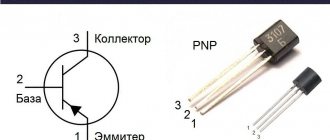
Bipolar
How to test a bipolar transistor with a multimeter? First of all, you need to find out which of the two subtypes - npn or pnp it belongs to. To do this, let’s remember what a bipolar transistor is.
This is a semiconductor element in which the so-called npn or pnp junction is implemented. Npn is the transition "electron - hole - electron", pnp, respectively, on the contrary, "hole - electron - hole".
Structurally, it consists of three parts - emitter, collector and base. In fact, a bipolar is two conjugated ordinary diodes, in which the base is the common connection point.
In the pnp circuit, the transistor differs from its npn counterpart in the direction of the arrow in the circle - the arrow of the emitter junction. For a pnp circuit it is directed towards the base, for an npn circuit it is directed vice versa.
You need to know this difference to check the bipolar transistor. A Pnp circuit is opened by applying a negative voltage to the base, and an Npn one by applying a positive voltage. But before this, it is necessary to find out which of the contacts of the transistor being tested is the base, which is the emitter, and which is the collector.
The instructions here could be as follows:
- the red (positive) probe is connected to the first terminal that comes across, for example the left one, the black (negative) probe alternately touches the central and right ones. Fix the value “1” on the central one, and 816 Ohms, for example, on the right;
- The red probe of the multimeter is short-circuited with the central contact, the black one - alternately with the side ones. The device displays “1” on the left and some value, say 807, on the right;
- when the red probe of the multimeter contacts the right terminal, and the black probe contacts the left and center, we get “1” in both cases. This means that the base is defined - this is the right contact of the transistor. And the transistor itself is PNP type.
In principle, this is enough to say that the transistor is working. Now, to check its structure and the specific location of the emitter and collector, we short-circuit the black (negative) probe of the multimeter with the base, and the red one in turn with the left and center contacts.
The contact that gives a lower resistance value will be a collector contact (in our case, 807 Ohms). The larger one - 816 Ohms - is the emitter one.
Testing an NPN type transistor occurs in the same way, only the positive contact is applied to the base.
This is a way to test pn junctions between base and collector and base and emitter. The multimeter readings may vary depending on the type of transistor, but will always be within the range of 500-1200 Ohms.
To complete the test, touch the emitter and collector probes. A working element will produce infinitely high resistance, regardless of its type, no matter how you change the polarity. If the value on the screen differs from “1”, one of the transitions is broken, the part is unusable.
Checking the built-in freewheeling diode
In almost any modern field-effect transistor, with the exception of special types, an internal “protection” diode is connected in parallel to the drain-source circuit. The presence of this diode inside the field device is due to the peculiarities of the technology for producing high-power transistors. Sometimes it interferes and is considered parasitic, but most field-effect transistors cannot do without it, as part of the integral structure of the electronic component.
Therefore, in a working field-effect transistor, this diode should also be working. In an n-channel field-effect transistor, this diode is connected with the cathode to the drain, and the anode to the source, and in a p-channel field-effect transistor, the anode is connected to the drain, and the cathode is connected to the source. Turn the multimeter into diode testing mode. If the field-effect transistor is n-channel, then attach the red probe of the multimeter to its source (source), and the black one to the drain (drain).
Transistors are one of the most widely used radioelements. Despite their reliability, they often fail due to irregularities in their operation. At the same time, searching for a faulty element due to the specific design of the field-effect transistor causes certain difficulties.
Typically the drain is in the middle and connected to the conductive substrate of the transistor, and the source is the right pin (check this in the datasheet). If the internal diode is working properly, the multimeter display will display a direct voltage drop across it - around 0.4-0.7 volts. If the position of the probes is now reversed, the device will show infinity. If everything is so, then the internal diode is working.
Measurement order.
Checking the drain-source circuit
The field effect transistor is controlled by the electric field of the gate. And if the gate-source capacitance is charged, then the conductivity in the drain-source direction will increase. So, if the transistor is n-channel, apply the black probe to the gate and the red one to the source, and after a second, reverse the orientation of the probes - red to the gate and black to the source. So we probably first discharged the shutter, and then charged it. The gate is usually on the left and the source is on the right.
Now move the red probe from the gate to the drain, and let the black probe remain at the source. If the transistor is working properly, then as soon as you move the red probe from the gate to the drain, the multimeter will show that there is a voltage drop at the drain - this means that the transistor has switched to a conducting state.
Now the red probe is on the source, and the black probe is on the gate (we discharge the gate with the opposite polarity), after which again the red probe is on the drain, and the black probe is on the source. The device should show infinity - the transistor has closed. For a p-channel field-effect transistor, the probes are simply swapped.
Checking the transistor without soldering.
If the device beeps
If at the drain-source testing stage the device beeps, this may be quite normal, because modern field-effect transistors have very low drain-source resistance when open. Alternatively, you can connect the gate to the source and in this position ring drain-source (for n-channel, red to drain, black to source), the device should show infinity.
The main thing is that there is no gate-source and drain-source ringing, especially at the moment when the gate is charged with the opposite polarity.