Let's talk about designing vias - for serious electronics their quality is very important. At the beginning of the article, I highlighted the factors that affect signal integrity, and then showed examples of calculating and tuning the impedance of single and differential vias.
Hello everyone, my name is Vyacheslav. I have been developing printed circuit boards for 5 years, and during this time I have not only read many rules and recommendations for routing, but also found primary sources and worked with them.
In complex computing systems that YADRO develops, high-speed signals travel significant distances on their way from transmitter to receiver, passing through several boards and making dozens of interlayer transitions. Under such conditions, each carelessly designed via will make a small contribution to signal degradation, and as a result the interface may not work.
Signal integrity
Via holes (hereinafter referred to as via) represent inhomogeneities in the transmission line.
Like other inhomogeneities, they spoil the signal. This effect is weakly expressed at low frequencies, but increases significantly with increasing frequency. Often, developers pay undeservedly little attention to the structure of vias: they can be copied from a “neighboring” project, taken from a datasheet, or not specified at all in CAD (the default setting). Before using the calculated structure, you need to understand why it was made that way? Blind repetition can only do harm.
The signal integrity of a channel as it passes through vias is primarily affected by the following factors:
- signal reflections due to changes in wave impedance;
- signal degradation due to parasitic capacitance and inductance;
- reflections from an unused segment of the p/o when moving to the inner layer (hereinafter stub from the English via stub);
- crosstalk (eng. Cross talks);
- interference in the power buses.
Let's take a closer look at the causes of these effects and methods for eliminating them.
Factor 1. Characteristic impedance p/o
In an ideally designed board, the wave impedance does not change throughout the entire route, including when moving to another layer. In reality it usually looks something like this:
Figure 1. Change in wave resistance when moving to another layer.
The better the wave impedances are matched, the less signal reflection will be. How can we influence this?
Let's consider the structure of the p/o on the board [1].
Figure 2. P/O structure on the board.
| Layer | Element | Property |
| TOP | P/o site | Parasitic capacitance between the pad and the L2 power supply area |
| TOP-L2 | section p/o | Inductance |
| L2 (power area) | Antipad | The anti-pad forms an edge capacitance - a capacitance between the walls of the p/o and the power supply area |
| L2-L3 | Section p/o | Inductance |
| L3 (power area) | Antipad | The anti-pad forms an edge capacitance - a capacitance between the walls of the p/o and the power supply area |
| L3-L4 | Section p/o | Inductance |
| L4 (signal) | P/o site | Parasitic capacitance between the power supply area and the L3 power supply area |
| L4-L5 | Stub | Noise Source |
By changing the elements of the junction, we change the characteristic impedance of the junction. Our goal is to match the impedance of the transition structure to the impedance of the conductors to minimize reflections. Let's consider how the impedance changes when the elements of the p/o structure change.
| Element | Action | Electrical property | Impedance (result) |
| P/o site | ↓ | C↓ | ↑ |
| Diameter of p/o | ↓ | L↑ | ↑ |
| Antipad | ↑ | C↓ | ↑ |
| Length | ↑ | L↑ | ↑ |
| Number of power supply polygons along the route | ↓ | C↓ | ↑ |
| Step p/o | ↑ | C↓ | ↑ |
| Distance to return points | ↑ | L↑ | ↑ |
| Number of returnable items | ↑ | L↓ | ↓ |
| Filling holes | Fill with resin (Dk↑) | C↑ | ↓ |
↑ Implementation
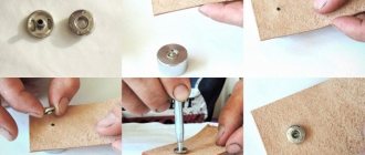
We insert the flared tube into the board. It is better if the hole in the PP corresponds as much as possible to the outer diameter of the tip tube; the tube should fit tightly, with difficulty. Press down as much as possible with your fingers. I did not use a special tubular upsetting with a hammer. The resulting margin resulting from incomplete contact of the flaring with the board is precisely used for flaring the rivet on the other side of the board.
We bite the rivet flush with the foil. As practice has shown, it is best to bite with side cutters with flat (without chamfer) cutting surfaces.
The tube naturally shrinks when cut, I tried, before biting, to insert a piece of winding wire inside the tube, but the result was not very foldable. It turned out that it was much easier to insert a suitable conical awl from the flaring side and straighten out this compression.
Factor 2. Parasitic inductance and capacitance
Conductors on a printed circuit board can be made with a characteristic impedance that lies in a wide range, but most often it is 50 Ohms.
On the one hand, this is due to historical continuity: 50 ohm impedance was standardized for coaxial cables as a compromise between driver load level and signal energy loss. On the other hand, a 50 ohm conductor is easy to fabricate on a standard board. What is important for the developer is not so much the specific value of the wave impedance, but rather its constancy throughout the entire transmission line.
In order to make a transmission line with a fixed characteristic impedance value, the designer selects the width of the track and the distance to the supporting layer, i.e. changes the linear capacitance and inductance of the transmission line to a certain
quantities.
In p/o the inductive component is quite significant. As a first approximation, we must, within reason, reduce the parasitic inductance as much as possible, and then change the p/o parameters to achieve the given
capacitance, and accordingly impedance.
An excessive decrease in the capacitance of the p/o will cause a local increase in impedance and, as a result, signal reflections.
NTD on metallization
According to IPC, H:d (aspect ratio) is defined as the ratio of the thickness (of printed circuit boards) to the minimum diameter of the drilled hole (drill diameter).
According to the domestic GOST 23 751 -86 - H:d (or the reciprocal value - γ) was defined as the ratio of the thickness (of printed circuit boards) to the minimum diameter of the metallized hole, i.e. at least 0.05 mm smaller (in GOST R 53429-2009, which replaced it), there is no mention of “aspect ratio” at all.
Note. Nevertheless, for a sufficiently deep understanding of the content of articles and documents, it is necessary to understand that the domestic standard corresponded to the smaller IPC standard, especially for small diameters (for example, H: d = 20: 1 or γ = 0.05 according to domestic technical specifications for a drill diameter of 0, 15 mm corresponds to H:d=13.5:1 according to IPC).
Another parameter characterizing the metallization of holes is the distribution of applied copper along the length of the hole (TP - English abbreviation). This parameter allows us to evaluate the ability of the plating process (especially for small hole diameters using direct plating) to deposit a sufficient thickness of the plating column without inadequately narrowing the lumen of the hole. Unfortunately, domestic normative and technical documentation does not specify this value in any way. In Fig. 94 shows two options for estimating the distribution:
— according to IPC – the most accurate;
— operational (TPMIN), often used by practicing technologists for quick assessment.
Figure 94. Options for calculating the distribution of metallization thickness
GOST 23752 specifies the minimum permissible average metallization thickness for double-sided printed circuit boards - 20 microns, for multilayer printed circuit boards - 25 microns.
Factor 3. Via stub
What happens when a signal passes through a stub via?
Figure 3. Via with stub, resonance at ¼ wavelength.
In our example, the signal propagates from top to bottom from the Top layer. Having reached the inner signal layer, the signal is split: part moves along the trace on the inner layer, and part continues to move down the via hole, then is reflected from the Bottom layer. After the reflected signal reaches the inner layer, it is again divided, part moves along the path, and part returns to the source.
The reflected signal will be added to the original signal and distort it, which will result in a narrowing of the window on the eye diagram and an increase in the level of insertion loss.
In the worst case, the TD segment will be equal to ¼ of the signal wavelength, then the reflected signal will reach the path on the inner layer with a delay of half a period, superimposing on the original signal in antiphase.
When analyzing integrity, it is recommended to consider a bandwidth of 5 Nyquist frequencies. A good approximation would be to consider a stub that gives resonance at the 7th harmonic and higher to be acceptable [2].
Figure 4. Insertion loss level graph for p/o with stubs 0, 0.65, 1.2 mm.
Figure 4 shows a huge resonance at frequencies around 24 GHz. We can conclude that if our signal operates at a frequency of 2–3 GHz, we can afford not to eliminate the stub, since within the 7th harmonics “everything is calm.”
You can quickly assess the criticality of a stub in the Polar calculator: Figure 5. Image from polarinstruments.com. A stub length of 2.5 mm is acceptable for signals with a rise time of more than 500 ps.
A slightly more accurate result is given by the formulas given in the article [2]. They take into account the geometry of the p/o and allow one to calculate a correction for the dielectric constant of the dielectric along the Z axis.
You can eliminate the stub using the “back drilling” operation, or using micro-vias (blind and buried vias). The choice depends on the characteristics of the project. Reverse drilling is easier and cheaper. After manufacturing the board, the stub is drilled to a given depth using a larger diameter drill. The developer is required to specify additional topology offsets in the drilling area, and it is also possible for the manufacturer to indicate drilling requirements in the design documentation. Modern CAD systems support this functionality.
Microvias are primarily intended for high-density boards (HDI), but in some cases they can be used, leveling out the high cost by eliminating back-drilling and reducing the number of layers on the board. There are some things to keep in mind when designing HDI boards:
- each new type of software increases the cost of the board;
- for laser drilling, special optimized prepregs are used, the properties of which may differ;
- Plating blind holes increases the thickness of copper on the inner layers.
It is highly recommended to agree on the board structure with the manufacturer in advance.
Metallization of vias in printed circuit boards (part 1, preparation of the activator)
- Store reviews (151)
I’ve been meaning to describe the metallization process in detail for a long time, but I still couldn’t complete the experiments with different additives to the activator (and their quantities), I licked all the technological steps.
Well, for some time I simply could not finally decide which option to describe. After some hesitation, I decided to describe the option with the addition of liquid soap. This option was chosen for two reasons: the reagents are more accessible and after thermolysis the workpiece is washed much easier. The second point is especially important in this technology, since it somehow didn’t make sense to install a second electroplating (although I tried this option of washing pyrolysis products “on my knees”). The downside is the need to activate quickly, but it’s hard to say whether this is a minus or a plus. So. A little insight into the theory, history and tribute to the people who made this method accessible to hobbyists. This method is based on the ability of some copper compounds to decompose under the influence of heat to release metallic copper. This method emerged as a result of work on palladium-free metallization technologies that began during the times of the former USSR. After the collapse of the USSR, work was not stopped and in the early 90s a group of chemists from the Novosibirsk Institute of Solid State Chemistry and Mechanochemistry, headed by Oleg Ivanovich Lomovsky, received the last patent for this technology. As a matter of fact, the method described below is only an adaptation of the technology described in the patent. Another person who needs to be given credit is user JIN from the vrtp.ru forum. It was he who made available to the masses of chemistry dummies, like me, an affordable way to obtain a base solution for the activator. Well, now that all the necessary curtsies have been made, I’ll move on to the technology itself. ATTENTION! ALL WORK ON PREPARING THE SOLUTION AND PROCESSING THE BOARD IS PERFORMED WITH GLOVES! During processing in the activator, it is strictly not recommended to touch the surface of the board, even if your hands are wearing gloves. This is about caring about the result, not about the hands. The activator does not contain highly toxic substances, but nevertheless it contains copper compounds, most of which are, at a minimum, not beneficial to health. Ammonia is also not good for health, so the activator should be stored in a sealed container, out of the reach of children and pets. To work, you will need the following reagents and instruments: Reagents : 1. Copper (II) sulfate (aka copper sulfate)
What you need is a reagent, pure (pure) or analytical grade (pure for analysis)
.
You can, of course, also have HF (chemically pure) or OSCh (extra pure), but I haven’t come across one like that. Vitriol that is sold in garden stores may contain an unknown amount of impurities.
2.
Calcium phosphate (aka calcium hypophosphite, aka calcium phosphinate). Also Ch or ChDA
(and, of course, chemically pure or high purity).
3. Distilled water. The one sold in car dealerships is quite suitable. 4. Ammonia water 25% (aka ammonia, aka ammonia hydrate, aka ammonium hydroxide). Pharmaceutical ammonia is also suitable, but you will have to pour more of it and adjust the amount of water (I didn’t count exactly how much, but I think everyone can handle this task from a school chemistry course). 5. Liquid soap. Any will do, but if possible, you should take one that contains fewer additives (it is usually also cheaper). It is also worth giving preference to soap with a neutral pH; such soap usually emphasizes this fact on the packaging. Tools and materials : 1. Household scales with a resolution of at least 1 gram (more precisely, in fact, it is not necessary). 2. Two containers in which the solution is prepared, glass or plastic. The capacity of the first is somewhere from a liter or more. The capacity of the second is about half a liter. 3. Plastic container with a tight-fitting lid. This will be the working container in which the activator is stored and in which the boards are processed. 4. Large funnel for pouring liquid, preferably plastic. 5. Several wet wipes for hands (if you have old dried ones, that’s even better). It is highly advisable to choose ones that do not contain any additives. Before use, wipes should be placed in a warm place and dried. These wipes will be used for filtration. Since there is a lot of sediment, regular paper napkins will not hold up. In addition, they absorb too much liquid and thus affect the composition, which is not desirable. 6. Large syringe 20 or (better) 60 ml. ATTENTION! The final stages of preparing the solution (starting from step 7) are best done outdoors or under a hood. Still, ammonia is pretty smelly. The prepared solution smells much less and can be used indoors. The solution is prepared as follows: (For those who have looked at other recipes, let me clarify that the recipe is “double” in the number of components; “single” is not enough for convenient work.) 1. Pour 140 ml of distilled water into the first container:
To speed up the next step, it is advisable to heat the water in the microwave to 35-40 degrees. 2. Pour in 30 grams of vitriol:
Then mix thoroughly until completely dissolved in water. When all the vitriol has dissolved, we get this blue liquid:
3. Pour in 22 grams of calcium hypophosphite:
And stir the resulting mixture for several minutes. The solution quickly becomes whitish; calcium sulfate (gypsum) is released, which is insoluble in water:
4. Place a funnel in the second container and place napkins in the funnel:
5. Carefully drain the liquid from the first container into the funnel. In this case, you need to periodically shake the sediment so that it does not remain in the first container. When filtering is finished we get this picture:
6. Pour 100 ml of water through the sediment. In this case, the sediment becomes slightly whiter. We wait until all the liquid has drained, remove the watering can and get a solution of copper hypophosphite in water:
7. Add 40 ml of ammonia water to the solution using a syringe. If the syringe is large, then this can be done in one go; with a 20, you will have to do two passes. It is most convenient to squeeze ammonia water into the solution by dipping the tip of the syringe directly into the solution, this avoids splashing. If you need to do two passes, then between passes the tip of the syringe should be rinsed in distilled water. The solution instantly thickens and white flakes appear in it:
Slowly stir the solution until the flakes completely disappear and the solution turns into a homogeneous dark blue liquid:
This solution already smells much less and the process can be continued indoors, if necessary. 8. Add 5-6 ml of liquid soap to the solution:
9. Add 8-10 grams of calcium hypophosphite to the solution:
Mix thoroughly again. Hypophosphite does not dissolve completely, but undissolved sediment is also needed; it will maintain the concentration of hypophosphite ions in the solution as it is used. Continuing to stir, pour the solution into the working container. In this case, you need to ensure that the sediment is completely poured along with the rest of the solution. The activator is ready. The activator is stable and can be stored for a long time. During use, you need to ensure that there is always a sediment of calcium hypophosphite at the bottom and, if necessary, add a couple of grams. If this is not done, unplated holes may appear. Read Part 2 (plating)
Author Sergiy Yevtushenko
Original article on the website https://we.easyelectronics.ru
Factor 4: Crosstalk
Crosstalk is the unwanted transmission of a signal from one line to another.
This transfer occurs because two closely spaced conductors have capacitive and inductive coupling. The nature of crosstalk between signal conductors and p/o is slightly different. In the s/o, the signal does not have a supporting layer; return currents flow through adjacent s/o, forming a large loop. Crosstalk of signals in the p/o is caused by the inductive component.
The greatest effect in minimizing crosstalk can be achieved by increasing the distance between the p/o. However, often the topologist does not have much space.
The proximity of the p/o in a differential pair not only reduces the occupied area, but also has a positive effect on noise immunity [3].
A common way to minimize crosstalk between adjacent signal terminals is to place a shielding terminal between them. With this method, you will need to conduct signals in increments of about 2 mm (Figure 6). If there is not enough space, you can use a smaller step with a shift (English Staggered pattern), as in Figure 7. Using simulation, you can select the ideal shear angle [4].
Figure 6. Minimizing crosstalk using shielding P/O.
Figure 7. Minimizing crosstalk using diagonal checkerboard shift.
Crosstalk can also be reduced by exotic methods, for example, a long stub (by shifting the inductive-capacitive balance of the p/o) [5]. Interference can also be reduced at the design stage of the chip package [6].
↑ Tool
Wire cutters, pliers, hole punch and hammer. A cone awl is an important tool in this matter. I had a drill sharpened in time immemorial (now I can’t even imagine why) - it just fit. Well, and most importantly, a multifunctional tool, commonly called a “tin can,” which plays the role of an anvil.
Experiments have shown that the result is quite functional, not factory-made, of course, but this does not matter - the uneven edges of the rivets are hidden under the solder.
Factor 5. Interference in the power buses
In addition to adjacent signal circuits, signal quality can be affected by interference from internal layers.
Large currents can flow through power supply areas. Due to the increase in inductance at the edges of the polygons, flowing currents form fringing fields along all boundaries of the polygon, including in cutouts. Edge fields are a source of electromagnetic radiation (edge-fired emission) into space. To reduce the emission of electromagnetic radiation, the 20H rule is applied (Figure 8), which consists of narrowing the power polygon in relation to the ground polygon.
Figure 8. Edge fields and the 20H rule.
To protect the power supply from interference, if possible, it is necessary to increase the anti-fall at power supply areas. The 20H rule for p/o is difficult to provide, and also unnecessary; an anti-pad with a diameter of about 2 mm is usually recommended (Figure 9).
Figure 9. Increased anti-fall on power layers
Chemical plating and direct metallization.
These chemical processes (they do not involve the influence of external current sources) form a conductive sublayer on the dielectric in the drilled holes, through which the galvanic build-up of copper is subsequently carried out. In this case, one of the main parameters of the printed circuit board is implemented: the ratio of the thickness of the printed circuit board to the minimum drilling diameter (H/d) when forming a sufficient thickness of a layer of ductile galvanic copper on the hole wall. In modern high-density precision printed circuit boards this ratio reaches 10...12/1 (and in the most complex printed circuit boards 20/1) for through holes and 1.0 - 1.2/1 (max 1.5/1) for blind holes. The main task that is performed as a result of these processes is the formation of reliable end contacts.
Fig.96. Chemical copper layer in the area of the end contact
During chemical copper plating at the end contact of a metallized hole on a printed circuit board, galvanic copper, formed during the metallization of the hole, comes into contact with the foil of the inner layers through a layer of chemical copper deposit. This layer is the weakest point. By its nature, chemically deposited copper has a loose porous structure that can absorb moisture, gases, electrolyte solutions and has low mechanical strength.
Destruction of the end contact under operational influences (mainly temperature, thermocyclic) occurs, as a rule, along the layer of chemical copper. One of the main conditions for the formation of a reliable end contact is the epitaxial splicing of the galvanic copper layer of the metallization column and the end of the foil, which is possible only through a layer of chemical copper with a thickness of no more than 0.8...1 microns (Fig. 96). Thus, when implementing the process of chemical copper plating, a rather difficult technological conflict arises:
- on the one hand, to reliably cover the entire surface of the hole post, you want to apply more chemical copper (make it thicker);
- on the other hand, the thickness of chemical copper to form a reliable end contact and ensure epitaxial splicing of the layer with the foil should not be more than 1-1.5 microns.
I don’t want to say that this conflict is unsolvable, but it requires a very deep study of the chemistry of the processes and significant efforts to maintain the composition of working solutions and modes at all stages of the process.
Fig.97. Adhesion failure on the surface of printed circuit boards associated with a thickened chemical copper layer. Violation of copper-to-copper adhesion
As an example, I can cite a situation that made an indelible impression on me, as a person who does not have a fundamental chemical education.
In the technical process of chemical metallization, according to which we worked for many years, copper ions were bound into complexes with the participation of Rochelle salt (potassium-sodium tartrate). As it turned out, the supplied salt may contain salts of several isomers of tartaric acid, only one of which is a complexing agent. Its mass fraction in the product produced in the Russian Federation is not regulated and therefore may change. However, the deposition rate, and therefore the thickness of the chemical copper layer, directly depends on the content of this particular isomer. With the delivery of each new batch of salt, problems began with the reliability of the end contacts. It took quite a lot of time and effort to understand the reasons and develop methods for incoming salt control. But this is just one example of one stage of a multi-stage complex process.
The adhesion problem associated with an increase in the thickness of the loose, mechanically weak, gas-filled layer of chemical copper manifests itself not only in the area of the end contact, but also over the entire surface of the conductors of the outer layer, since the chemical copper layer lies wherever galvanic copper is applied to the foil (Fig. 97).
Additional disadvantages of chemical copper plating include the presence in the working solutions and, consequently, in the drains of harmful (with very low maximum permissible concentrations), difficult to extract substances (formalin, Rochelle salt, EDTA, etc.).
Direct metallization is devoid of the main disadvantage of chemical copper plating - the presence of an additional layer between the foil and galvanic copper. The conductive sublayer formed during direct metallization at the final stage of the process lies only on the dielectric. Naturally, provided that it is implemented correctly (Fig. 98).
Fig.98. Epitaxial splicing, through direct metallization in the area of the end contact
In addition, the advantages of direct metallization include the absence of hydrogen evolution (“pitting”), which leads to the formation of metallization defects in holes, especially small diameter ones. Another advantage is the ability to implement the direct metallization process on high-performance conveyor units.
The transition from chemical to direct metallization does not necessarily involve the purchase of a new line. Since the direct metallization process has fewer stages, chemical metallization lines are sufficient to implement this process.
Existing direct metallization processes can be divided into 3 types based on the type of conductive layers formed. Let me give a brief summary of their characteristics:
1. Graphite-based conductive layer. Mainly used for double-sided printed circuit boards. The technical process is compact, cheap, and highly productive. The essence of the process is the processing of printed circuit boards in a fine suspension of graphite. Graphite particles, having sizes from several tens to several hundred nm, are adsorbed on the surface being treated and, after drying, acquire conductivity due to the presence of a metallic bond between carbon atoms. Carbon particles are removed from the copper surface by microetching.
The advantages of graphite-based processes include their simplicity, compactness, relative cheapness, and high productivity. The success of the process largely depends on the uniform distribution of particle sizes in the suspension. In other words, the particles should be predominantly the same size. However, during the operation of the suspension, they stick together and become larger. Such enlarged particles give a loose, exfoliating sediment. The adhesion of galvanic copper to it is insufficient. Therefore, it is periodically necessary to analyze the graphite suspension, which requires appropriate equipment. The technological window of a process that provides sufficiently high reliability is very narrow, which requires frequent adjustments and increases the cost of this operation. Therefore, the process is used, as a rule, for the production of double-sided printed circuit boards and multilayer printed circuit boards for household appliances used in equipment with a short life cycle.
Fig.99. Separating layer in the area of the end contact in case of violation of the intermediate flushing technology
2. Conductive layer based on palladium. This method is most common for the manufacture of multilayer printed circuit boards, including special applications. His idea is that already at the activation stage, palladium is so dispersed over the surface that it forms a continuous conductive (with semiconductor conductivity) film without the subsequent stage of chemical deposition of copper.
There are technical processes for palladium direct metallization with different mechanisms for the formation of colloidal solutions. In this case, the adsorption of micelles or a promoter layer occurs both on the dielectric and on copper, and requires the removal of these layers from the copper surface by active washing and microetching so that no separating layer remains between the foil and galvanic copper (Fig. 99).
Distribution (the ratio of the thickness of copper in the center to the thickness at the entrance to the hole) in direct metallization processes is no more than 75%. Reliably implemented H:d (aspect ratio) for through holes is 8:1, for blind holes – 1.2:1.
3. Conductive layer based on a conductive polymer.
Conductivity in this method is created by polymerization of monomers of organic substances, and due to the nature of the polymerization process, conductivity occurs only in the dielectric areas inside the hole. This method does not require a micro-etching step or intermediate rinsing, and therefore conductive polymer processes provide high Cu-Cu bond strength at the end contacts that persists after repeated thermal exposure. However, the conductivity of these layers is also comparable in magnitude to the conductivity of layers based on graphite and Pd sulfide. This method is promising, innovative, but little developed abroad. And it has not been mastered at all in the Russian Federation.
Summarizing the above, the advantages of direct metallization include:
- 1. Absence of formaldehyde and strong complexing agents in working solutions.
- 2. Short time for creating surface conductivity of the dielectric - ~15 sec.
- 3. The solutions used are highly stable and do not require “overclocking” after technological breaks.
- 4. Absence of a separating layer in the end contact.
- 5. Possibility of creating surface conductivity for a wide range of DE.
- 6. Satisfactory dissipation power for H:d≤10 for through holes.
- 7. Less volume of chemical analyses.
- 8. There is no copper in plums.
What to choose: chemical copper or direct metallization?
If the process of chemical copper plating is mastered, stable, understandable and works normally for a long time, apparently, one should follow the recommendation: “They don’t look for good from good.” If we are talking about modernization or the creation of a new production, and the planned range and production volumes of printed circuit boards require a significant reduction in production costs, and the design of the produced printed circuit boards (primarily H:d) allows the use of direct metallization, then it is probably worth focusing on one of the direct metallization processes.
It should be taken into account that the conductive layers of preliminary metallization, formed by all three previously described methods of direct metallization, have a relatively small thickness and semiconductor conductivity, while a further increase in thickness during the galvanic process occurs from the entrance to the hole to its middle. Which limits the maximum achievable distribution of copper and, accordingly, the maximum achievable H:d.
Some palladium direct metallization processes make it possible to increase the conductivity of the preliminary metallization layer by increasing the density of seeding the dielectric surface with palladium micelles. This somewhat improves the distribution of copper in the hole, but at the same time increases the consumption of palladium and, at the same time, does not allow achieving the conductivity of chemical copper. So, with chemical copper technology, the preliminary metallization layer has metallic conductivity and further thickness increases in the direction perpendicular to the walls of the hole. This makes it possible to realize high values of the copper distribution parameter in the hole and, accordingly, to realize significantly higher H:d values than with direct metallization.
Currently, in the production of multilayer printed circuit boards, both chemical copper plating and direct metallization are used to create a conductive layer in the holes. The conductivity of the dielectric walls of the holes is created already at the activation stage, which is present both in the process of chemical copper plating and in the process of direct metallization. However, in the direct metallization process, the stage of chemical deposition of copper is eliminated. In this regard, direct metallization does not have the disadvantages inherent in chemical copper, and is, of course, preferable for simple multilayer printed circuit boards with H:d up to 10:1. The continued use of electrochemical copper plating for the manufacture of relatively simple multilayer printed circuit boards is largely due to the conservatism of manufacturers and their reluctance to abandon a well-established process.
At the same time, in most industries, especially those that care about the prospects for their development, it seems advisable to adopt the following organizational strategy at the electroplating stage:
Technological approaches
Since the ratio of printed circuit boards with large and small H:d (aspect ratio), respectively, is ≈20%/80%, it is advisable to have 2 metallization lines:
High-performance - with direct metallization (palladium or conductive polymers) for printed circuit boards with “small” H:d≤ 8:1 (i.e. for the production of large quantities of relatively simple printed circuit boards). Such a line will support the ongoing program and can be the basis of contract manufacturing.
Relatively low-productivity - with chemical copper, with galvanic filling of holes, for printed circuit boards with “large” H:d (up to 20:1), vibration, airless mixing (Venturi nozzles), forced supply of solution over the workpiece area (for the manufacture of complex, innovative, but quite expensive printed circuit boards). Such a line will allow developers to implement innovative ideas and will shorten the prototyping cycle and the implementation time for new developments in general.
Calculating the impedance of single vias
Based on knowledge of the influence of p/o elements on impedance, we can design our ideal p/o.
A great place to start is to calculate the impedance in a calculator. Among engineers involved in the development of printed circuit boards, calculators such as the Saturn PCB Design Toolkit and Polar Instruments Si9000e are popular. Both of them allow you to quickly calculate the impedance of a single p/o.
The results obtained in these calculators are very different from each other. This is because these tools have different approaches.
Polar calculates impedance in a two-dimensional plane where the p/o intersects the power polygon. No calculation formula is provided. It was experimentally established that the calculation is made using the formula for the impedance of a coaxial cable:
Figure 10. Image from polarinstruments.com
The illustration shows a rather low value of dielectric constant Er1 compared to the standard one. This is due to the heterogeneity of the dielectric structure: it consists of resin (Er 3.2) and fiberglass strands (Er 6.1), therefore it has an average dielectric constant of about 4.1. This value can vary quite a lot locally. Thus, near the p/o, resin predominates, so the value of the dielectric constant is recalculated downwards [7].
Saturn PCB calculates impedance using the formula:
When the length of the p/o changes, the values of inductance and capacitance change disproportionately, and the impedance changes. The impedance of exactly the same 1.6 mm long p/o is calculated by the Saturn PCB as 128 Ohms! (Figure 11)
Figure 11. Calculation of p/o in the Saturn PCB Design Toolkit program.
The question immediately arises: who to believe?
Let's model in a three-dimensional electromagnetic field solver (English 3D Solver) how it will look on a real 8-layer board with a thickness of 1.6 mm (Figure 12)
Figure 12. Transition structure between layers with a hole for return current.
In our case, the impedance turned out to be about 70 Ohms. By bringing the return voltage closer, you can achieve a reduction of another 5 ohms. By “playing” with the size of the anti-pad, you can quite accurately adjust the impedance to the target value (Figure 13).
Figure 13. Impedance of a circuit with a p/o on a timing diagram.
In the frequency domain, “better” parameters are expressed in a lower reflection coefficient from the input (Figure 14).
Figure 14. Parameters of single p/o in the frequency domain.
Polar's calculation turned out to be closer to the result obtained. It is possible that to obtain an adequate result in the Saturn PCB, it is necessary to introduce corrections. If anyone has a positive experience with impedance calculations on a Saturn, please share in the comments!
Manual method of applying PCB tracks
Preparing the template
The paper on which the printed circuit board layout is drawn is usually thin and for more accurate drilling of holes, especially when using a hand-made homemade drill, so that the drill does not lead to the side, it is necessary to make it thicker. To do this, you need to glue the printed circuit board design onto thicker paper or thin thick cardboard using any glue, such as PVA or Moment.
Next, the thick paper is cut out along the contour of the glued pattern and the template for drilling is ready.
Cutting the workpiece
A blank of foil fiberglass laminate of a suitable size is selected, the printed circuit board template is applied to the blank and outlined around the perimeter with a marker, a soft pencil or marking with a sharp object.
Next, the fiberglass laminate is cut along the marked lines using metal scissors or sawed out with a hacksaw. Scissors cut faster and there is no dust. But we must take into account that when cutting with scissors, fiberglass is strongly bent, which somewhat worsens the adhesion strength of copper foil and if the elements need to be re-soldered, the tracks may peel off. Therefore, if the board is large and has very thin traces, then it is better to cut it using a hacksaw.
The template of the printed circuit board pattern is glued to the cut-out workpiece using Moment glue, four drops of which are applied to the corners of the workpiece.
Since the glue sets in just a few minutes, you can immediately begin drilling holes for radio components.
Calculating the impedance of differential vias
The calculation of differential p/o is similar to single ones, except that now we do not have a calculator: the above tools do not calculate differential p/o.
Also, now we can additionally change the step p/o in differential. couple Let's take the same structure: an 8-layer board with a thickness of 1.6 mm. Let's consider 9 p/o configurations (Figure 15).
The first 3 p/o have gaps of 0.125 mm and differ only in the location of the holes for the return current. All p/o from 4 onwards have a pitch of 1 mm. P/o from 6 onwards have an increased anti-fall (0.250 mm) and differ in the indentation of the holes for the return current.
Figure 15. Vias.
Consider the impedance graph (Figure 16).
Figure 16. S/O impedance in the time domain.
The “hump” is clearly visible on the graph, which corresponds to the vertical segment of the p/o - “glass” (English: Via barrel).
Having examined the frequency dependence of the reflection coefficient of VIA1-3 (Figure 17), we see that despite good performance at the target frequency of 6 GHz, there is resonance at lower frequencies. It is preferable to improve via7-9, and if that doesn’t work, then via4-5 in order to reduce the “hump” by shifting the graphs to the right.
Figure 17. Reflection coefficient from the p/o input.
Let's reduce the anti-fall on VIA9 to get gaps of 0.125 mm. For VIA4, let’s reduce the p/o step to 0.75 mm and consider the result obtained (Figure 18).
Figure 18. Impedance comparison of modified p/o.
In the frequency domain, a shift of the reflection coefficient graph from the input to the right is visible (Figure 19).
Figure 19. Comparison of reflectance of modified p/o.
Final Recommendations
Vias in printed circuit boards are a complex and heterogeneous structure.
To correctly calculate parameters, expensive 3D solvers, competencies and significant time are required. If it is not possible to avoid the use of transitions of critical signals to other layers, it is necessary first of all to assess the degree of influence of the resulting inhomogeneities on the integrity of the signals. If the inhomogeneity is electrically short (delay time less than 1/6 of the edge), the stub resonates at frequencies outside the passband - there is no point in wasting time and money on optimization.
As a first approximation, it is convenient to use ready-made structures from datasheets or previous boards, but remember the features of the current project.
Calculators allow you to quickly estimate the parameters of the software, but they use highly simplified models that negatively affect the result.
Bibliography
- Chin, T. Differential pairs: four things you need to know about vias. Retrieved from TI E2E Community: https://e2e.ti.com/blogs_/b/analogwire/archive/2015/06/10/differential-pairs-four-things-you-need-to-know-about-vias#
- Simonovich, B. Via Stubs Demystified. Retrieved from Bert Simonovich's Design Notes: https://blog.lamsimenterprises.com/2017/03/08/via-stubs-demystified/
- Demystifying Vias in High-Speed PCB Design. Retrieved from Keysight Technology: https://www.keysight.com
- K. Aihara, J. Buan, A. Nagao, T. Takada and C. C. Huang, “Minimizing differential crosstalk of vias for high-speed data transmission,” in Proc. 14th Elect. Perform. Electron. Packages and Systems, Portland, OR, Oct. 2014.
- C. M. Nieh and J. Park, “Far-end Crosstalk Cancellation using Via Stub for DDR4 Memory Channel,” in Proc. 63rd Electronics Components and Technology Conference, Las Vegas, NV, May 2013, pp. 2035-2040.
- H. Kanno, H. Ogura and K. Takahashi, “Surface-mountable Liquid Crystal Polymer Package with Vertical Via Transition Compensating Wire Inductance up to V-band,” in IEEE MTT-S Int. Microwave Symp. Dig., Philadelphia, PA, June 2003, pp. 1159-1162.
- Via Pad / Anti-Pad Impedance Calculation. Retrieved from Polar instruments https://www.polarinstruments.com/support/si/AP8178.html
