Greetings, friends!
We have already talked about how some of the “building blocks” from which computers and peripheral devices are made work.
Those who like to dig deeper read here how transistors and diodes work.
Now we’ll look at what other gizmos manufacturers are cramming into electronic equipment.
To begin with, we note that technical progress also means reducing the size of electronic components.
What are SMD components
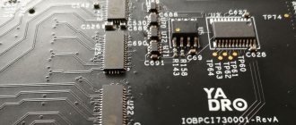
SMD components are used in absolutely all modern electronics. SMD ( Surface Mounted Device English means “surface mounted device”. In our case, the surface is a printed circuit board, without through holes for radio elements:
In this case, SMD components are not inserted into the holes of the boards. They are soldered onto contact tracks, which are located directly on the surface of the printed circuit board. The photo below shows tin-colored contact pads on a mobile phone board that previously had SMD components.
Home page
SMD is a mounted device installed using surface mount technology.
SMT is surface mounting technology for electronic components and devices.
DIP is a technology for mounting electronic components in holes.
BGA is a type of electronic component package with leads formed on the bottom side in the form of a matrix.
SOT (SOD) - Small Outline Transistor (Diode) - literally translated means 'transistor (diode) with small leads'. At the present stage, not only transistors and diodes are placed in SOT-type cases, but also transistors with resistors, zener diodes, voltage regulators based on an operational amplifier, and much more, and the number of pins can be more than three.
Surface Mount Component Housings.
Many companies produce elements in housings that do not meet international standards. There are also situations when a body that has standard dimensions has a non-standard name. Often the name of the case consists of four numbers that indicate its length and width. But in some standards these parameters are specified in inches, and in others in millimeters. For example, the name of the 0805 package is as follows: 0805 = length x width = (0.08 x 0.05) inches, and the 5845 package has dimensions of (5.8 x 4.5) mm: Cases with the same name can have different heights, different contact pads and made of various materials, but designed for installation in a standard installation location. Below are the dimensions in millimeters of the most popular types of housings.
| Type of shell | L* | W* (mm) | H** (mm) | k (mm) | Note |
| 0402(1005) | 1.0 | 0.5 | 0.35…0.55 | 0.2 | |
| 0603 (1608) | 1.6 | 0.8 | 0.45…0.95 | 0.3 | |
| 0805 (2012) | 2.0 | 1.25 | 0.4…1.6 | 0.5 | GOST PI-12-0.062 |
| 1206 (3216) | 3.2 | 1.6 | 0.4…1.75 | 0.5 | GOSTP1-12-0.125; P1-16 |
| 1210 (3225) | 3.2 | 2.5 | 0.55…1.9 | 0.5 | |
| 1218 (3245) | 3.2 | 4.5 | 0.55…1.9 | 0.5 | |
| 1806 (4516) | 4.5 | 1.6 | 1.6 | 0.5 | |
| 1808 (4520) | 4.5 | 2.0 | 2.0 | 0.5 | |
| 1812 (4532) | 4.5 | 3.2 | 0.6…2.3 | 0.5 | |
| 2010 (5025) | 5.0 | 2.5 | 0.55 | 0.5 | |
| 2220 (5750) | 5.7 | 5.0 | 1.7 | 0.5 | |
| 2225 (5763) | 5.7 | 6.3 | 2.0 | 0.5 | |
| 2512 (6432) | 6.4 | 3.2 | 2.0 | 0.6 | |
| 2824 (7161) | 7.1 | 6.1 | 3.9 | 0.5 | |
| 3225 (8063) | 8.0 | 6.3 | 3.2 | 0.5 | |
| 4030 | 10.2 | 7.6 | 3.9 | 0.5 | |
| 4032 | 10.2 | 8.0 | 3.2 | 0.5 | |
| 5040 | 12.7 | 10.2 | 4.8 | 0.5 | |
| 6054 | 15.2 | 13.7 | 4.8 | 0.5 |
| Type of shell | L* (mm) | W* (mm) | H** (mm) | F (mm) | Note |
| 2012 (0805) | 2.0 | 1.2 | 1.2 | 1.1 | EIAJ |
| 3216 (1206) | 3.2 | 1.6 | 1.6 | 1.2 | EIAJ |
| 3216L | 3.2 | 1.6 | 1.2 | 1.2 | EIAJ |
| 3528 | 3.5 | 2.8 | 1.9 | 2.2 | EIAJ |
| 3528L | 3.5 | 2.8 | 1.2 | 2.2 | EIAJ |
| 5832 | 5.8 | 3.2 | 1.5 | 2.2 | — |
| 5845 | 5.8 | 4.5 | 3.1 | 2.2 | EIAJ |
| 6032 | 6.0 | 3.2 | 2.5 | 2.2 | EIAJ |
| 7343 | 7.3 | 4.3 | 2.8 | 2.4 | EIAJ |
| 7343Н | 7.3 | 4.3 | 4.3 | 2.4 | EIAJ |
| DO-214AA | 5.4 | 3.6 | 2.3 | 2.05 | JEDEC |
| DO-214AB | 7.95 | 5.9 | 2.3 | 3.0 | JEDEC |
| DO-214AC | 5.2 | 2.6 | 2.4 | 1.4 | JEDEC |
| DO-2 IVA | 5.25 | 2.6 | 2.95 | 1.3 | JEDEC |
| SMA | 5.2 | 2.6 | 2.3 | 1.45 | MOTOROLA |
| SMB | 5.4 | 3.6 | 2.3 | 2.05 | MOTOROLA |
| SMC | 7.95 | 5.9 | 2.3 | 3.0 | MOTOROLA |
| SOD 6 | 5.5 | 3.8 | 2.5 | 2.2 | ST |
| SOD 15 | 7.8 | 5.0 | 2.8 | 3.0 | ST |
| Type of shell | L* (mm) | L1* (mm) | W* (mm) | H** (mm) | B (mm) | Note |
| DO-215AA | 4.3 | 6.2 | 3.6 | 2.3 | 2.05 | JEDEC |
| D0-215AB | 6.85 | 9.9 | 5.9 | 2.3 | 3.0 | JEDEC |
| DO-215AC | 4.3 | 6.1 | 2.6 | 2.4 | 1.4 | JEDEC |
| DO-21SBA | 4.45 | 6.2 | 2.6 | 2.95 | 1.3 | JEDEC |
| ESC | 1.2 | 1.6 | 0.8 | 0.6 | 0.3 | TOSHIBA |
| SOD-123 | 2.7 | 3.7 | 1.55 | 1.35 | 0.6 | PHILIPS |
| SOD-323 | 1.7 | 2.5 | 1.25 | 1.0 | 0.3 | PHILIPS |
| SSC | 1.3 | 2.1 | 0.8 | 0.8 | 0.3 | TOSHIBA |
| Type of shell | L* (mm) | D* (mm) | F* (mm) | S* (mm) | Note |
| DO-213AA (SOD80) | 3.5 | 1.65 | 048 | 0.03 | JEDEC |
| DO-213AB (MELF) | 5.0 | 2.52 | 0.48 | 0.03 | JEDEC |
| DO-213AC | 3.45 | 1.4 | 0.42 | — | JEDEC |
| ERD03LL | 1.6 |
Pros of SMD components
The biggest advantage of SMD components is their small size. The photo below shows simple resistors and SMD resistors:
Thanks to the small dimensions of SMD components, developers have the opportunity to place a larger number of components per unit area than simple output radio elements. Consequently, the installation density increases and, as a result, the dimensions of electronic devices decrease. Since the weight of an SMD component is many times lighter than the weight of the same simple output radio element, the weight of the radio equipment will also be many times lighter.
Simple radioelements always have parasitic parameters. This could be parasitic inductance or capacitance. Here, for example, is the equivalent circuit of a simple capacitor, where the dielectric resistance between the plates, R is the resistance of the leads, L is the inductance between the leads.
In SMD components these parameters are minimized, because their dimensions are very small. As a result, the quality of transmission of weak signals is improved, and less interference occurs in high-frequency circuits due to lower values of parasitic parameters.
SMD components are much easier to desolder. For this we need a soldering station with a hair dryer. You can read how to desolder and solder SMD components in the article on how to properly solder SMDs. It's much more difficult to seal them. In factories, special robots place them on a printed circuit board. No one solders them manually in production, except for radio amateurs and radio equipment repairmen.
Selecting soldering paste
The quality of any flux is expressed in the fact that during soldering it does not burn out, it only barely evaporates, and the products of its decomposition are easily removed with a solvent. The best flux is special pastes. We chose the top names based on the experience of familiar masters:
- Interflux 2005 and 8300
- Kingbo RMA-218
- Amtech RMA-223
- Rexant BGA and SMD flux gel
Just in case, keep in mind the old, “old-fashioned” ways of finding flux in a remote village. This is an aspirin tablet, fruit juice, olive oil, ammonia with glycerin, rosin with alcohol. The most obvious one for rural areas is pine or spruce resin. You need to melt the resin over low heat and then pour it into matchboxes.
Main types of SMD components
Let's look at the main SMD elements used in our modern devices. Resistors, capacitors, low-value inductors, fuses, diodes and other components look like ordinary small rectangles, or rather, parallelepipeds))
On boards without a circuit, it is impossible to know whether it is a resistor, a capacitor, or even a coil. The Chinese mark as they please. On large SMD elements, they still put a code or numbers to determine their identity and value. In the photo below these elements are marked in a red rectangle. Without a diagram, it is impossible to say what type of radio elements they belong to, as well as their rating.
The standard sizes of SMD components may be different. Here is a description of the standard sizes for resistors and capacitors. Here, for example, is a yellow rectangular SMD capacitor. They are also called tantalum or simply tantalum:
And this is what SMD transistors look like:
There are also these types of SMD transistors:
Inductors, which have a high rating, in SMD version look like this:
And of course, how can we live without microcircuits in our age of microelectronics! There are many SMD types of chip packages, but I divide them mainly into two groups:
1) Microcircuits in which the pins are parallel to the printed circuit board and are located on both sides or along the perimeter.
2) Microcircuits in which the pins are located under the microcircuit itself. This is a special class of microcircuits called BGA (from the English Ball grid array
- an array of balls). The terminals of such microcircuits are simple solder balls of the same size.
The photo below shows a BGA chip and its reverse side, consisting of ball pins.
BGA chips are convenient for manufacturers because they greatly save space on the printed circuit board, because there can be thousands of such balls under any BGA chip. This makes life much easier for manufacturers, but does not make life any easier for repairmen.
Semiconductor markings
Accurate information is applied to the device body so that the buyer can immediately determine which device is in front of him
This is important, given that inside one case there may be small parts with different parameters
Therefore, they pay attention to identifying SMD components by their markings
Diodes
Usually they are supplied with color markings. At least if the body is cylindrical. Products are marked with colored stripes, in quantities of one or two pieces. The strips are easy to find at the cathode terminal, which is supplied to the diodes.
In a rectangular case, devices are equipped with approximately the same designations. Some manufacturers include different symbols and numbers in their designations.
Zener diodes
Their markings are both color and symbolic. The marking strips are also located closer to the zener diode terminals.
Circuit breakers
LEDs
Typically, SMD LEDs are not provided with additional markings. An exception is for counterfeit goods of low quality. They are often marked with different symbols to make the product look more convincing. There are digital symbols, but they are only needed to see the size of the device. All other information is placed in the accompanying documents. The requirements for marking foreign SMD diodes are set a little differently.
The main thing is to take into account that some devices can be produced in different modifications, with some differences in the main characteristics. Even with the same standard size, different LEDs differ in color and color temperature.
What services does the contract installation company provide?
Using the services of a contract assembly company can bring a number of benefits to many entrepreneurs in a variety of industries, such as cosmetics, medical, construction, appliances and electronics, or automotive. Third party contract assembly services improve product quality by:
- application of innovative and precise technologies;
- availability of specialized production lines;
- employment of experienced specialists.
On the other hand, entrepreneurs using contract assembly services can increase profits not only by bringing cutting-edge technology solutions to market, but also by not having to maintain their own production line in the face of rapidly changing technology.
About multilayer boards
Installation in equipment with SMD components is often quite tight. Therefore, the boards themselves need more tracks so that no problems arise during further operation. All the tracks cannot fit onto one surface, which is why a multilayer version of the boards was developed.
The board will have more layers if the equipment itself is quite complex. The tracks themselves are located right inside the board; it is almost impossible to see them. Computer and mobile phone boards are an example of the use of such technologies in practice.
Note! When multilayer boards overheat, they simply swell like a bubble. Interlayer bonds begin to break, causing the main component to fail
Proper temperature is the most important factor in any repair.
Sometimes both sides of the printed circuit board are used for work. Because of this, the installation density becomes twice as large. Another advantage of modern SMT technologies. The material for the production of such components also requires several times less. Thanks to this design, the cost is reduced.
Valid schemes
Metallization of holes
The ductility of copper deposits should be correlated with the thermal expansion of the base of the boards along the Z axis. It will be clearly greater at higher soldering temperatures with lead-free solders. To resist the expansion of the base and ensure greater strength and greater ductility of copper deposits, it is necessary to more tightly control the plating process of through holes. To ensure heating of through mounting holes to higher temperatures typical of lead-free soldering, it is necessary to ensure appropriate thermal conductivity of the metallization by increasing its thickness. All this forces us to reconsider the requirements for the technology of metallization of printed circuit board holes.
#3 – Excessive solder
Excess solder accumulates at this joint, notice the round shape. (on the picture). If your board went through wave soldering equipment and required too much solder, then you will get excess buildup
If your board went through wave soldering equipment and required too much solder, then you will get excess buildup.
Notice the rounded shape in the picture and although this excess solder can still form an electrical connection, it becomes difficult to determine what is happening inside this rounded mass. Reasons for over soldering can be due to the following reasons:
Reasons for over soldering can be due to the following reasons:
- Incorrect orientation of components of the same type in the same direction.
- Using the wrong lead length to site ratio during your design process.
- On the manufacturer's side, the conveyor belt may have been running too fast.
Work related to connecting LEDs and other elements
Modern electronic devices are equipped with leadless SMD components. Their circuit does not provide for the presence of wire leads. The connection occurs by soldering the contact surfaces. For work, use a 10-12 W soldering iron, connecting each contact in series.
https://youtube.com/watch?v=0b_Xo5H7IBg
When soldering the SMD element, the terminals are heated. For a soldering iron, you need to make several tips with branches at the end. When using a more powerful tool, several turns are made on the tip using copper wire, forming a convenient attachment. It allows you to quickly desolder SMD components. The nozzle is dismantled and used as an alternative to a low-power soldering iron for connecting thin conductors to LEDs. When soldering such tape (to protect the printed track), soldering should be done in a very short time.