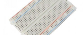
Solderless breadboard
The design of this type of breadboard is simple. Its basis is a plastic case with a large number of holes on the top plane. The holes contain contact connectors for installing parts. The connectors allow the installation of contacts and wires with a diameter of up to 0.7 mm, the distance between them is standard 2.54 mm, which allows the installation of transistors and microcircuits in DIP packages.
The connectors are connected to each other in a special way - in vertical rows of 5 pieces, and many boards also have dedicated power buses - in them, the connectors are connected along the entire length of the board (horizontally), and are marked with blue (-) and red (+) lines. Physically, the connectors and buses are made in the form of metal contacts inserted into the back of the board and covered with a protective sticker.
There are solderless breadboards of different sizes - from 105 to 2500 or more contact points. For convenience, a coordinate grid can be applied to the board. Many boards are designed like a construction kit - several pieces can be assembled into one large board, which allows you to prototype designs in modules.
Additional tools
What is not in the set, but will or may be needed:
1. Tweezers. We took a manicure. 2. 9V Krona battery 3. Phillips screwdriver - one of the circuits has a terminal. Tighten the wires in it using a clockwise Phillips screwdriver. 4. A “third hand” soldering device - this is something you can do without, although it is constantly mentioned in the instructions and brochure. Of course, it would be more convenient with it, but if you simply assemble all the parts on the board and then turn it over, then both boards included in the set will be relatively stable and soldering will be, in principle, convenient and without additional devices. 5. Magnifying glass 6. Desalter pump 7. Goggles and respirator 8. Soldering iron stand 9. Fan/exhaust hood
Of this entire list, it will be very difficult only without the first two points. This time our stand for the soldering iron was the robot from the previous post. The rest for mounting two small boards would really be superfluous.
But it would be useful to remind you that when soldering, tin vapors are released, which are not very beneficial for health. Actually soldering the two circuits included in the kit took me no more than 10 minutes and I didn’t feel bad. However, a small fan to push the smoke away, or at least an open window, is standard and very good practice. In addition, you should wash your hands after soldering. You also need to take care of your eyes - the leg of a part bitten off by wire cutters may fly off, or a drop of hot tin may fly off during the soldering process (although it didn’t fly off for us). Therefore, wear safety glasses. Take care of yourself!
Printed breadboards
Such boards are designed similarly to printed circuit boards, but with the only difference: the prototyping board contains either a grid of holes with a distance of 2.54 mm (with or without contact pads), or a standard pattern (for example, for prototyping devices on microcircuits), or both another at once. Moreover, there are single-sided and double-sided boards.
Disposable circuit boards
Circuit board is a universal printed circuit board for assembling and modeling prototypes of electronic devices. There are single-sided and double-sided in different sizes. The holes are very conveniently matched to the sizes of the pins of the microcircuits, as well as other radio elements. Therefore, it is very convenient to assemble and test electronic devices on such breadboards.
The reverse side of such development boards with ready-made devices will look something like this:
What are the disadvantages of circuit boards? It is still better to use them once, since with repeated use their spots may fly off, which will lead to their unsuitability.
Solderless breadboards
There are many types of solderless breadboards. They differ in the number of pins, number of buses, and configuration. But they are all arranged according to the same principle. A development board consists of a plastic base with many holes, usually spaced at a standard 2.54mm pitch. The legs of the output microcircuits are usually located with the same pitch.
The holes are needed to insert the leads of radio elements or connecting wires into them. A typical view of a breadboard is shown in the figure.
The picture below shows a breadboard with the base at the bottom removed. As you can see, the board has rows of metal plates .
Each metal plate looks like the figure below. That is, it is not just a plate, but a plate with clips that are hidden in the plastic part of the circuit board. It is into these clips that you connect your wires.
That is, as soon as you connect a conductor to one of the holes in a separate row, this contact will be simultaneously connected to the other contacts in a separate row.
Please note that there are five clips on one rail . This is the generally accepted standard. Most solderless breadboards are implemented this way. That is, you can connect up to five components inclusive to a separate rail on the breadboard and they will be interconnected. But there are ten holes in a row on the board! Why are we limited to five contacts? You probably noticed that in the center of the circuit board there is a separate rail without pins? This rail isolates the plates from each other .
The picture below shows an LED mounted on a solderless breadboard. Note that the two LED legs are mounted on insulated parallel rails. As a result, there will be no contact closure.
Now let's look at larger breadboards.
On such boards, as a rule, two vertically located rails are provided. The so-called power rails .
These rails are similar in design to horizontal ones, but are connected to each other along the entire length. When developing a project, you often need power for many components. It is these rails that are used for power supply. Usually they are o and “-” and in two different colors - red and blue . As a rule, the rails are connected to each other to get the same power on both sides of the breadboard (see the figure below). By the way, there is no need to connect the plus specifically to the rail marked “+” , this is only a hint that will help you structure your project.
A pinless center rail insulates the two sides of the solderless circuit board. Besides insulation, this rail has a second important function. Most integrated circuits (ICs) are manufactured in standard sizes. In order for them to take up minimal space on the circuit board, a special form factor is used called Dual in-line Package, or DIP .
DIP chips have contacts located on both sides and fit perfectly on two rails in the center of the breadboard. It is in this case that contact insulation is an excellent option, which allows you to route each contact of the microcircuit onto a separate rail with five contacts.
The figure below shows the installation of two DIP chips. Above is the LM358, below is the ATMega328 microcontroller, which is used in many Arduino boards.
You've probably noticed that solderless circuit boards have numbers and letters near the rows (horizontal rails) and columns (vertical rails). These markings are provided for convenience only. The prototypes of your devices very quickly become overgrown with additional components, and one error in the connection leads to the inoperability of the electrical circuit or even to the failure of individual components. It is much easier to connect a contact to a rail, which is marked with a number and a letter, than to count the contacts “by eye”.
When you're designing an electrical circuit, you don't have to limit yourself to just one breadboard. Many circuit boards have special grooves and tabs on the sides. With these slots, you can connect several breadboards and create the workspace you need. The picture below shows four solderless breadboards connected together.
Some solderless circuit boards have a self-adhesive backing on the back . A very useful feature if you want to securely install the breadboard on some surface.
On some large breadboards, the vertical rails that receive power consist of two parts that are isolated from each other (for example, an 830-pin breadboard).
It is very convenient if your project needs two different power sources: for example, 3.3 V and 5 V.
But you need to be extremely careful and before using the breadboard, connect one power source and check the voltage at the two ends of the vertical rail using a multimeter.
Printed and solderless breadboard: how to use?
Installation on a breadboard without soldering comes down to installing parts into connectors and connecting them with jumpers (special or homemade). It should be remembered that the connectors in the lines are connected and an error can lead to a short circuit.
There is no need to explain how to use a breadboard for soldering: just insert the parts into the holes and solder them to each other and to the jumpers. But soldering should be done carefully, since frequent overheating causes the contact pads and traces to peel off from the board.
Purpose
I would like it to be possible to run any real microcontroller on a breadboard - one that will later be used in a real device (without migrating to another “stone”, which involves additional murky steps and is fraught with glitches). I’m still a beginner in microelectronics: I still don’t have enough design experience to take into account all the nuances and easily present a portable program (and now, I program in assembler - this tightens the development conditions and makes it very difficult to migrate the firmware to another MK!)
- therefore, everything needs to work and be debugged immediately “specifically and transparently.”
In world practice, it is often recommended: to wire up a microcontroller with all the wiring - directly on a contact breadboard - here it is convenient to connect any peripherals... the question is, what else is needed? But this is the first method with which I generally began experiments with microcontrollers - but due to bad contacts, not a single circuit worked for me at all! Or only the first one and a half launches worked. The programmer was terribly buggy: the microcontrollers were not flashed at all, or were flashed with glitches, verification failed - so I quickly ruined all my stones (for some reason, with the nth unsuccessful firmware, their “fuses” got lost, although I didn’t even touch them, and the microcontroller no longer started). “Stones” were revived with “high-voltage programming” (here, they helped me a lot: a spare programmer in the “STK500”, and smoking manuals). But the stones “died” on the breadboard again, very soon...
DI HALT also wrote that he does not use "pin breadboards" for prototyping, for similar reasons of "bad contacts", but only uses "breadboards that are soldered". This is perhaps the only correct solution in this case: since at high frequencies (on the order of megahertz), at which microcontrollers operate and the programmer transmits signals, a clear low-impedance contact, as well as communication lines with low capacitance, are absolutely necessary!
So, at least the most critical part of the board (microcontroller with wiring and programmer connection) must be made on soldered contacts
— so that programming and debugging work without glitches, so that the “heart of the circuit” works. And the periphery can already be separated and separated on a temporary “breadboard with holes”, and connected with wires to the main soldered breadboard with a microcontroller - this is a solution of sufficient reliability and good flexibility...
Which development board should I choose?
The easiest to use is a solderless board, which is why it is very popular today, and even novice radio amateurs know how to work with a solderless breadboard. In addition, the boards are durable and very reliable. Printed circuit boards are more difficult to work with because they require soldering, but they have the important advantage that they can be used to prototype the final installation on a permanent printed circuit board.
Therefore, it would be a good idea to have both types of breadboards and use them depending on the situation. Oh yes, and you can buy breadboards here.
From n/a Vladimir Vasiliev
PS Friends, be sure to subscribe to updates! By subscribing, you will receive new materials directly to your email! And by the way, everyone who signs up will receive a useful gift!
Nutrition
To begin with, all we need is a separately purchased Krona battery. The kit has a connector for it, which, according to the instructions, must be soldered into the first circuit. My advice: don't do this, leave it like that and use it in both schemes - both to test the first and to configure the second.
The devices that we will assemble consume some insane amount of mAh.
If we are talking about an electrical circuit, then our resources and how we quickly spend them are measured in A/h (Ampere per hour, mAh). Capacity of a typical “Krona” (according to the passport):
625 mAh ≈ 0.5 Ah
The first device, Chameleon, consumes up to 200 mAh. Therefore, our Krona for this scheme will be enough for:
625mAh/200mA = 3.125 hours.
which means it is recommended to use it only to check the operation of the circuit. A good solution would be a 12 volt battery with a capacity of at least 0.5 Ah.
mAh is how quickly the battery runs out! =)
It would be cool to be able to solder one of these connectors onto the boards, and then plug in a lab power supply like this. But there are no suitable holes for any of the available connectors on the board. Therefore, we cannot connect the power supply yet.
Historical excursion
In the early 1960s, chip prototyping looked something like this:
Metal stands were installed on the platform, on which conductors were wound. The prototyping process was quite long and complex. But humanity does not stand still and a more elegant approach was invented: Carefree breadboards!
If you know that bread is translated as bread, and board is a board, then one of the associations that may arise when mentioning the word breadboard is a wooden stand on which bread is cut (as in the figure below). In principle, you are not far from the truth.
So where did this name come from - breadboard? Years ago, when electronic components were large and clunky, many DIYers in their garages assembled circuits using bread slicers (an example is shown in the picture below).
Gradually, electronic components became smaller and it was possible to reduce prototyping to the use of more or less standard conductors, connectors and microcircuits. The approach has changed somewhat, but the name has migrated.
Breadboard is a solderless circuit board. This is a great platform for developing prototypes or temporary circuits without the need for a soldering iron and all the hassle and time-consuming desoldering that comes with it.
Prototyping is the process of developing and testing a model of your future device. If you don't know how your device will behave under certain specified conditions, it is better to first create a prototype and test its performance.
Solderless circuit boards are used both for creating simple electrical circuits and for complex prototypes.
Another area of application for breadboards is testing new parts and components, such as microcircuits (ICs).
As mentioned above, the electrical circuit you create may well change and this is the main advantage of using solderless circuit boards. For example, at any time you can include an additional LED in the circuit, which will respond to certain conditions in your circuit. The figure below shows an example circuit diagram for testing the functionality of the Atmega chip, which is used in Arduino Uno boards.